If you have spent any time around I2C, you will have seen a plethora of diagrams about how the protocol works. The two primary forms are a traditional timing diagram or some representation of the bit stream in a timing-independent way. This one leans into the latter but also has some mix between a control flow diagram and a state transition diagram.

This is one of a series of diagrams handling read and write flows for controller and target devices.
The PCA9564 is a parallel to I2C interface chip. Most small devices these days do not expose a parallel interface, unlike older MPUs and MCUs. An I2C or TWI peripheral on-board is quite common; if not, then two GPIO pins can be bit-banged. However, for a device like an MC68000, which had limited on-chip peripherals but did expose its address and data bus, the PCA9564 and others of its kind were necessary devices. The 16550 was a similar device for providing UART functionality to an MPU. The PCA9564 is still available but looks pretty much end-of-life. I am not thinking of using one any time soon, but I am putting together some educational material and thought this device would be interesting to discuss. Last updated in 2006, the datasheet makes for some interesting reading, especially in the diagrams.
We can clearly see how the transactions are composed; we can see here the sequence of the components, START(S), TARGET 7-BIT ADDRESS (SLA), READ/WRITE# (W), ACK (A), DATA and STOP(P).
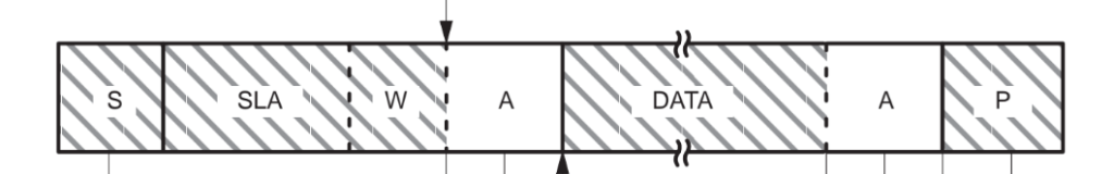
This is a very typical representation. Sometimes, the SLA and DATA are represented in a way which shows the bit ordering. There is no timing information here, but we don’t need that unless we are bit-banging. Since this documentation is for an interface chip that takes care of timing for us, that is irrelevant to our application. Of course, if we make a custom device at the other end of the link, we must know what timing to expect from this device. Timing diagrams are more useful when looking at a START, REPEATED START, STOP and BYTE(with ACK) timing, and not so much for a whole transaction.
One thing that is a little obscured here is that DATA is one or more bytes. The timing break, the two vertical wiggles, do not really show that it is alternating between TX BYTE and ACK, showing only a single ACK before the STOP. Still, that is not the motivation behind this diagram.
The diagram really is about state transitions. How you send or receive on an I2C bus depends on where ACKs do and don’t appear. The PCA9564 can work in multi-controller systems, so the state also depends on arbitration. You can see arrows showing a flow in this diagram. Closer inspection shows these to be state transitions.

There are some ways this diagram fails. Looking at the top row, “Successful transmission”, you can see state transitions at the end of the WRITE command flag. The forks are
- FAILED ARBITRATION – Halt and yield bus
- CHECK ACK
- ACK – continue transmission
- NACK – send STOP
The implication, and maybe the implementation, is to make this determination at the end of the ACK phase, and there is genuinely a three-way fork. This is to guide the user of the interface chip, so it makes a bit more sense in that context; the state values shown will be reported in the I2CSTA register when an interrupt occurs and will be the actual state.
The problem with this representation is that the arbitration lost, NACK and ACK conditions are three states that can follow the addressing phase. The Arrow from Addressing to NACK and a second arrow from NACK to ARBITRATION LOST can infer a sequence rather than optional states.
The second weakness is how each row seems to have commonality, but not necessarily. The row for ARBITRATION LOST has two contexts in which we can detect a bus conflict – during addressing and data transmission. There is one caption that applies to the whole width of the diagram. If we look back a few rows to the NACK (NOT ACKNOWLEDGED), we have two graphics, one showing that after a NACK, we send a STOP or a STOP is sent for us, the other, well, that’s actually about our options after REPEATED START.
How can this second problem be fixed? If there was a bounding box around the condition and what it applied to, that would help. The diagram is already busy enough, so that may not help, especially if colour is not an option.
Despite the shortcomings, I like this representation of what I2C transaction attempts can look like. The coupling of the phases of the transaction with the hardware state in this diagram shows when rather than just how the states can occur. This diagram aligns neatly with what we observe on our logic analyzer or oscilloscope. All potential “tail end” results are shown concurrently, rather than on separate timing diagrams, potentially on different App Note or User Manual pages. Even if the actual state numbers are different from your implementation, this diagram is generic enough to guide you through implementation or debugging.

One thought on “I think I’ve found my favourite I2C diagram”