Come on Alex, what’s so special about a debug UART? It’s just two pins on your board, that we hook up to our PC.
- The Debug UART Port
- Anatomy of a Debug UART
- The Problems
- You Can’t Plug USB in the Wrong Way
- Who is Perfect?
- About This Blog Post
The Debug UART Port
For those who deal with embedded systems, you know how much we rely on a serial connection to monitor our system and drive test stimuli into it. We need it to be a rock solid connection, though often it is not as solid as we like.
For those who aren’t in the trade, the debug UART port is a critical umbilical test harness used throughout the industry. As we develop an embedded system (your TV remote controller, your car stereo, your smart fridge display screen), we need to make sure our software and hardware are working properly together. How this universal tool is implemented varies; there are design tradeoffs made. Such tradeoffs can happen on any sub-circuit in an embedded system; indeed, tradeoffs are made in all walks of life.
Let’s identify the keywords, and then I’ll talk about how to get the perfect debug port.
- debug- removing faults from a hardware and software design
- port – a connection to an electronics device
- e.g. USB port, HDMI port
- debug port – a port used for debug data
- actually, the debug port is also used in development
- sometimes called the “console port”, which implies bi-directional communications, adding control.
- UART – universal asynchronous receiver/transmitter
- A device that allows data to be sent and received without a synchronization signal (clock) being sent alongside.
- Sometimes you’ll see USART (universal synchronous/asynchronous receiver transmitter), which can operate in a mode with a shared clock for synchronous transmissions.
- Serial – one bit after another, nothing happening in parallel.
- A way of sending data between devices while reducing the number of connecting wires.
- DUT – device under test
- Okay, that’s a term I haven’t used up to now; it’s the target hardware you are developing for and testing on.
Debug ports are very often implemented using a UART for serial communications. This is not the only way, some are implemented over different interfaces:
- JTAG
- Ethernet
- SWD
- Bluetooth
- WiFi
- USB
I’ll be focussing on the UART today as it is one of the most basic and prevalent forms we use. I will also be focussing on the electronic and mechanical side of it. In 30 years of industry, I’ve lost too many hours to loose connections and reversed signals.
Okay, now we all know the language. Now let’s look at the port in detail, then we will look at common problems and suggested best practices to limit the problems.
Anatomy of a Debug UART
UARTs are both very simple and extremely complex.
Externally, they look simple. You have two data lines, namely transmit (TX or TXD) and receive (RX or RXD), and then you have a shared ground. This means that you will have three header posts on your board, or some other connector to mate your DUT to your development PC.
When I was young(er), our development machines used to have what were called RS-232 ports; these were UART ports that operated at about 12V levels. Today, UARTS operate at around 3.3V, and development machines don’t have RS-232, but they do have USB. Thankfully, USB to UART cables and devices are available. You may hear the term “dongle” used to refer to them. One thing that was good about RS-232 was how it usually connected with a very solid physical connector, the D-sub. The two main connectors were the DB-25 and the smaller DE-9 (aka DB9 – see here for proper misuse).
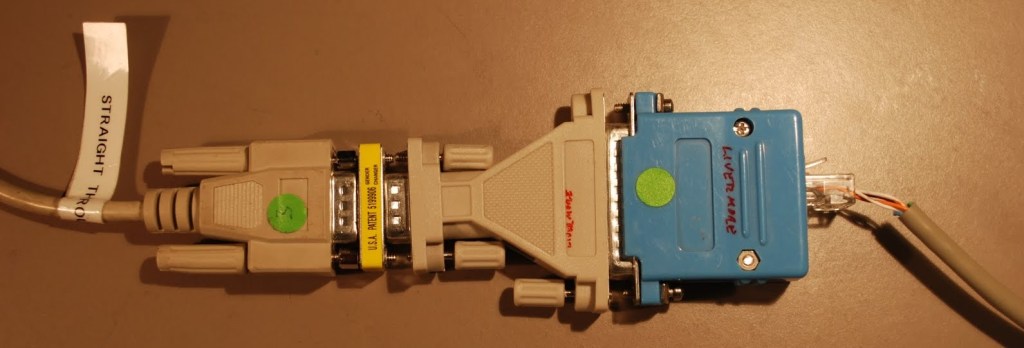
3ft DE-9F to DE-9M cable, F-F “gender changer”,
DE-9M to DB-25F, custom DB-25M to RJ45 patch box,
RJ45 crossover cable.
When we used RS-232, we all knew what voltage levels were expected. Often on the board there was a TTL to RS-232 level translation device (a charge pump, such as the MAX202). Occasionally, to reduce the BoM (bill of material) cost, the debug port would be raw TTL (5v) and we would need an external charge pump.
For the longest while, debug UARTS had been implemented using 3.3V devices, but with newer technologies we are seeing levels such as 1.8V, 1.2V, and even 1.0V. You have to match your USB-UART cable to these levels.
Another complexity, hidden during debugging, might be the use of an opto-isolator. This is simply a protection circuit that stops any high voltages from getting to delicate components on the DUT. It doesn’t impact debug, but you may see it when looking at the schematics.
As I said before, debug ports are both simple and complex. In hardware, the only complexity is matching voltage levels and hooking up the two data lines the right way around. In software, we have more fun (complexity). UARTs can send bytes of varying sizes. 8-bit data transfers are the most common, but you do sometimes see 7. Though 1 start bit is common, the number of stop bits can be 1, 1.5, or 2. Then, there is a confidence checker known as the parity bit. The parity bit can be turned off or can be set to odd or even. This basically shows if we have an odd or even number of bits set (value 1) in the byte.
The final parameter in software is the baud rate, that is, how many symbols per second can be sent. By symbol we mean a bit, but these include the start, stop, and parity bits as well as the data values. Baud rates have a series of typical values used. In times gone by 4800, 9600, and 19200 were common. The speed I personally see most often now is 115,200.
To summarize
- Hardware
- TX, RX data lines
- Ground
- Must know voltage level
- Software
- data size (number of bits)
- parity (none, odd, even)
- stop bits (1, 1.5, 2)
- baud rate
The Problems
There are three main problems.
- TX/RX reversed
- Wires don’t stay connected
- Compatible voltage level
Okay, these are broad, sweeping statements. It really depends on how your board was designed as to how much of a problem this will be, and it also depends on what USB-UART cable or connector you bring to the party.
The following image is not an advert, but a quick view of what USB-UARTs you may find out in the wild.

You have a choice between a cable, terminating in connectors that mate to header posts, or modules that will mount to headers. In the screenshot above, you will see the FTDI RPi and Adafruit terminate in 3 or 4 loose single-pole female sockets. Then we have the modules with pads, through-holes, posts, or sockets.
We also have the FTDI cable terminating in a 6-position socket. This is my personal favorite, but it can only be used on boards that are designed for it. Other USB-UART cables can just be added to your tool kit and used anywhere. I am not alone in thinking the FTDI TTL-234X-3V3 is a good choice; it is the serial device used with the BeagleBone Black. The FTDI RPi is designed for users of the Raspberry Pi.
Physical fit
My biggest gripe about modern debug ports is the physical fit and how well the wires stay connected. You will often find two posts, TX and RX, close to each other. The board designer may have placed a ground close by for you, or there may be a bank of grounds a few inches away.
With the connectors that rely on several single-pole female sockets mating to posts, you will find that the sockets wear loose over time, especially with many insertions. The mechanical shields are sized to allow easy connection and removal without any pressure causing the posts to deform. Between the wear on the socket or a cheap post that’s a little thinner, the connector can easily work loose. This is always exacerbated when your DUT gets jostled on your bench, particularly when probing the board with your scope or hooking up a logic analyzer on other posts around your debug port.

Strain relief can help with this. You can see in the photo above I have my DUT mounted to a carrier board. The FTDI RPi cable is also tied to the carrier, as is the other data cable. The downward and sideward forces make sure my cable does not work loose. You can see both a zip tie and ladder tie in use. Ladder ties are wonderful for temporary connections, though they often don’t snug up as tight against smaller cables. You want enough tension so the connector doesn’t work loose, without damaging the board or cable.
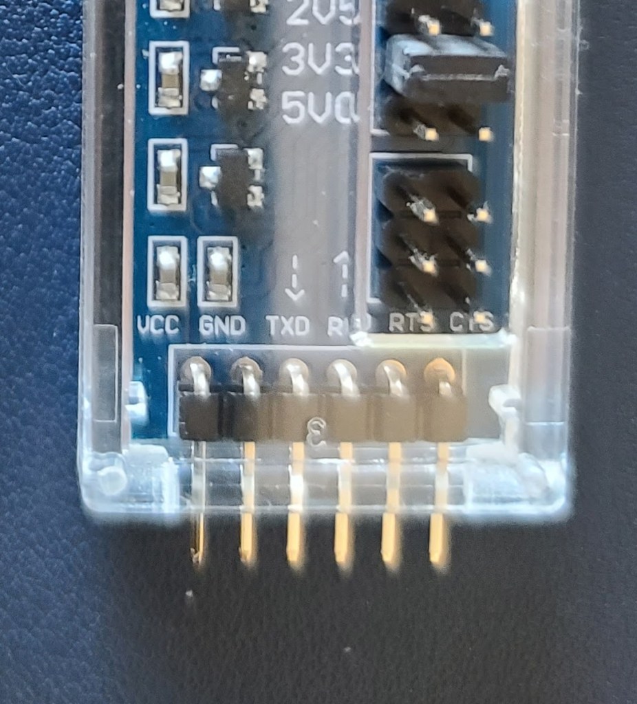
The FTDI TTL-234X-3V3 has a fuller connector. Not only are TX, RX, and ground provided, but so are VCC (power), and two flow control signals, CTS# (Clear to send) and RTS# (request to send). This six-pin socket provides a secure physical connection. I have never had one of these work loose.
TX/RX reversal
You would think this would be simple. But I’ve watched people get it wrong for 30 years, and 30 years ago I bought a book, “The RS-232 Solution,” which documented how people had been getting this wrong for a decade before I started my first professional job.
It used to be that you had two types of equipment on a serial connection:
- DTE – data terminating equipment
- Computer, TTY terminal
- Source/destination for data
- DCE – data communications equipment
- Modem
- A communications relay device
Two DTEs would connect with a pair of DCEs in between, providing a communications bridge. The simplest form of DCE was a “NULL MODEM,” essentially a patch box or cable that would provide crossovers of key signals, TX-RX, DTR-DSR, and CTS-RTS. DTR (data terminal ready) and DSR (data set ready) are extra handshake lines from the DTE and DCE, respectively. Not mentioned yet is DCD (data carrier detect), which meant the DCE pair had a valid bridge between them. In a Null modem, this typically gets ganged to DSR, as it is part of the DCE-ready status. The null modem replaces the pair of DCE devices.
Why was the knowledge of DTE versus DSE so important? Well, the DTE TXD connects to the DCE TXD, and DTE RXD connects to DCE RXD. The crossover of TX and RX happened in the communications link. It’s analogous to a phone conversation; the participants are the DTEs and the phones are the DCEs. Everyone speaks into a mouthpiece (TX) and listens to an earpiece (RX). If a null modem was present, it routed DTE1 TXD to DTE2 RXD and DTE2 TXD to DTE1 RXD.
In the world of debug ports, do we label the port relative to the debug PC or to the host MCU onboard?
The USB UART connector is always labeled as if it were the PC acting as a DTE. That is what it is, so it should look that way. PC out is TX, PC in is RX.
The MCU, or microcontroller, is also a DTE. Its own UART ports are labeled TX for out and RX for in. If the hardware engineer labels the signal traces from those ports across the schematic, then they will logically be labeled TX and RX, respectively, matching the port pin assignments.
Now, how should we label the debug header? This always causes discussion in the schematic reviews and, ultimately, confusion on the bench. In the last few teams I was in, it was decided for the silk screen to show the naming of the PCs USB UART, making sure the DUT at the board level used DCE naming. This gives us a null modem on the board. It makes things simple, you hook ground to ground, TX to TX, and RX to RX. However, you can’t protect yourself from clever teammates; They all know that the USB-UARTs TX needs to hook to your MCU’s RX and vice versa. So they swap. Everyone has a 50% chance of getting it wrong, but it’s easy to swap those two fly leads. If we’d named it the other way round, well, everyone knows you hook TX to TX, etc. You can’t win on naming alone.
I know on some boards the space for the silkscreen layer is limited, but directional arrows can help. If you look at the DCD-Tech USB-UART dongles, you will see arrows pointing on or off the board. This direction is easy to see as they are labeling 90° connectors, not vertical.
The main thing is to be consistent in naming. If you can, have a “best practice” or policy for this so that the debug port is named consistently across all your projects. You may have new hires from elsewhere who will see you are doing it differently from elsewhere, but at least you will be common within the organization.
Descriptive text in the schematic can be very helpful. Tell the reviewers in simple human language what the pins are for in a comment block, something like the following:
| Pin | Usage |
| DEBUG_TX | Data transmitted from PC to MCU UART RX |
| DEBUG_RX | Data from MCU UART TXC to PC RX |
Bonus points if your breakout, or debug board can accommodate that in its silkscreen.
The FTDI 6-pin Cable
The hard one is when it comes to that fancy 6-pin FTDI cable. I know I was pushing this as the best for a mechanical solution, but this one is harder to fix if you get wrong on the schematic.
I was at a company that had made the mistake of swapping the TX and RX. In the lab were several modified cables that would work, but those cables were now dedicated to that vintage of the board. Should the next rev board maintain this setup? It would allow swapping between the rev A and rev B boards, but, topic for another blog, you should limit the number of vintages you have loose in the lab.
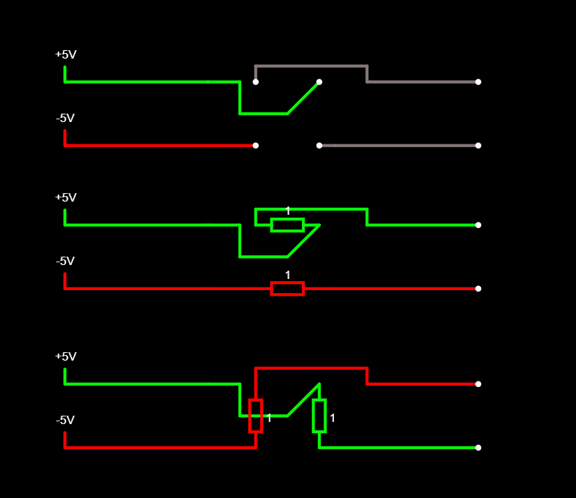
I later learned the trick to successfully designing the multi-pin UART connector. You make it repairable in HW. It’s a neat trick, really. You use stuffing options of zero ohm resistors, or solder blobs to chose a pair of data paths. The pads have to be laid out in a square to do this.
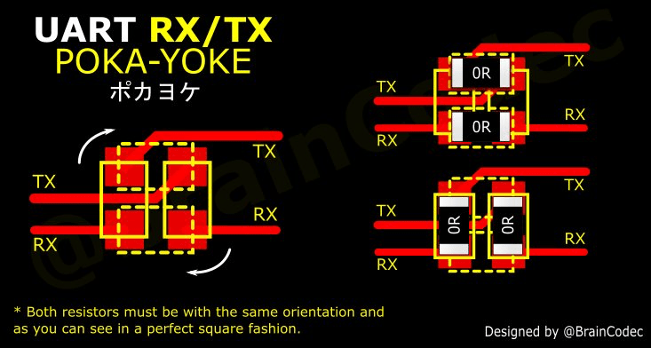
You will see some resemblance to a bridge rectifier, and I personally would rather lay this out in a diamond fashion.
Also, I’m bold enough to believe I have it right, so I would add cuttable traces on the top layer for the default path. If I get it wrong, I can cut and jump, but if I got it right, I saved stuffing a couple of 0-ohm resistors. I guess it all depends on the volume you are building, and who is doing the rework.
This same trick can be applied to the CTS and RTS signals if they are used. In many cases, though, flow control is not used, and the user should disable host PC hardware flow control in their terminal program.
The Busy, Crowded Board
I am a big fan of the clever placement of debug headers. I like the headers around the edge of the board. This gives me the most room to reach in with the probes for my multimeter, or my oscilloscope.
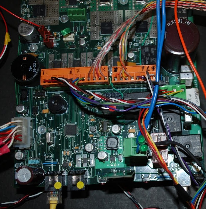
This controller card from a limousine, pictured below, shows how cabling can obscure a significant portion of the board. Some debug headers have to be in the midst of a rat’s nest like this in order to meet signal integrity or timing constraints, but the fewer there are, the better.
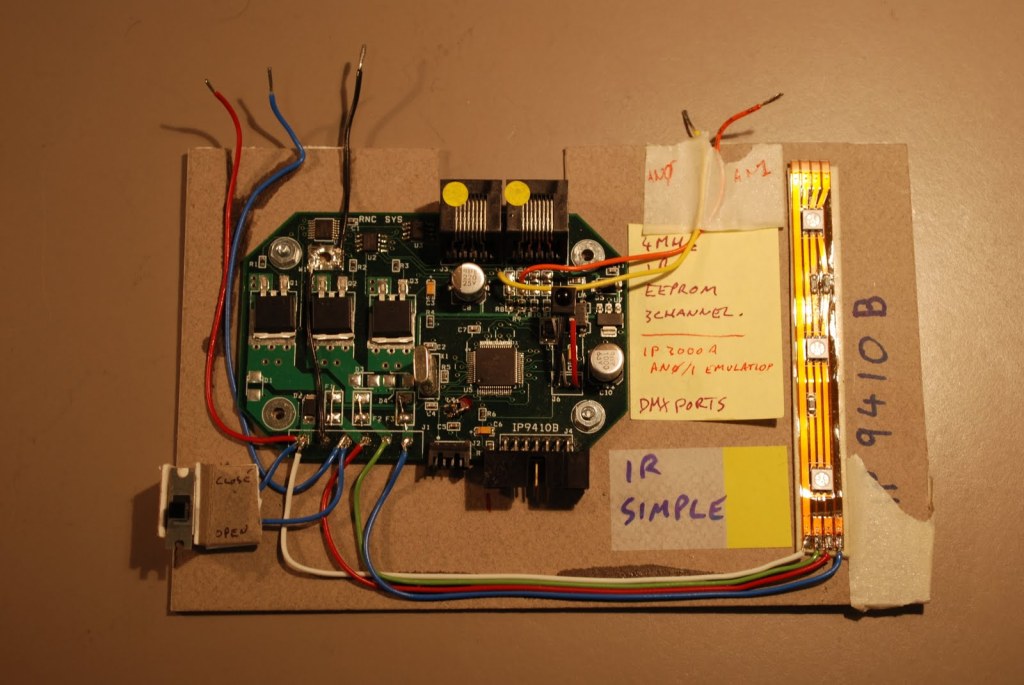
The use of right-angle connectors is a blessing and a curse. They increase the footprint needed for your DUT, but they also don’t crowd your airspace. Cables that run planar to your board can easily be clamped to a carrier board. I’ve used sheet metal, plexiglass, pegboard, and even cardboard to provide a stable base. The below Izinagi light controller was mounted on card using a mix of double-sided tape, hot-glue, and CA glue. Masking tape was used to hold the board to my bench. You can see the whole board and easily probe anywhere.
You Can’t Plug USB in the Wrong Way
So, if you want to make sure the correct USB to UART interface is used. That is, matched voltage, correct orientation, all the signals. Why not use a module on your board?

I have seen this done, and do always propose it as a candidate if appropriate. You will see that we have a complex system; the red board is our main board, the blue board, I forget the exact nature of it. The silk screen suggests that it was our debug board; if it was an EVK, that also makes sense. For this context, though, what is important is that we see the two modules in the upper right corner. They are UART or DUART (Dual UART) modules. I would suspect at that company, we were using FTDI devices, but I had previously seen the same with SiLabs modules. These were hard soldered down for reliability but could have been socketed for flexibility.
You would use this solution for a non-form factor board of a small device or the companion debug board for a small form factor DUT. If your final form factor is a large board, then you could do this on your main board. It is a no-stuff item until needed, reducing cost.
I like this for its ruggedness and ease of use. You never have to wonder what the voltage is or where you left the cable. All you need is the correct length USB cable with the appropriate connector. USB micro B and Type C connectors fit with a positive action, and are hard to accidentally dislodge.
I will admit, though, that it looks like a “blue wire special.” You will see a TX/RX pair from one of the modules to the IC. They are potted on well with hot glue. It looks like that vintage design had TX and RX swapped, hence the cut and jump. Nobody’s perfect.
Arduinos, Espressif’s ESP32-Devki C, and many ST and Atmel EVKs use a similar solution to this. They multiplex the ICE debug port, such as SWD or JTAG, alongside the console port into a single USB interface.
Who is Perfect?
We just said, “Nobody’s perfect,” but by being aware of common pitfalls, we can make life easier for ourselves. It’s the team’s responsibility to make the right choices for the project. Between the hardware and software engineer, you will find the best solution. It will be a compromise, but make sure you have considered all the following.
- Ease of use:
- (Nearly) fool proof connection
- Secure fitting
- Simple, meaningful silkscreen
- Consistent naming on schematic
- Location:
- Not cluttering interesting board areas
- Not crowding airspace
- You’re not unplugging this one every five minutes – keep it out of harms way.
- You don’t want it too buried though – you will quickly need it when problems occur.
- Design rules:
- Don’t compromise on signal integrity
- No antennas
- No cross-coupling
- Don’t compromise on signal integrity
- Cost:
- Look for test equipment that can be re-used later
- Look for solutions cheap enough you can build in
I have probably missed some key points, but I hope I’ve got you thinking about how your debug UART port could be implemented better. There’s nothing worse than trying to debug a device with intermittent debug connections. If you have ideas or best practices of your own, I’d love to hear them.
About This Blog Post
Image Credits
- Photos by me
- For layout diagram
- For resistor block paths
These links were both found in the Reddit discussion at https://www.reddit.com/r/PrintedCircuitBoard/comments/s4s7nx/design_trick_to_swap_two_signals_with_resistor/
AI Usage
I usually use ChatGPT for several iterations of review. However, I have a family member who vehemently objects to the use of AI in any form. They have suggested I get a human to review my work. That’s all well and good if I had a volunteer co-contributor, or I was monetizing this blog and could pay someone.
As part of my on-going investigation on how AI can help me, I’ve decided to rely on my own review abilities, and use a robotic spelling and grammar checker, not an AI based grammar checker. Let’s see if it hurts my readership any.
Updated March 2025
I’ve noticed this is one of my more popular posts. I reviewed it to see why it’s so popular, and in doing so, I found a few issues to fix. The fixes were only in language: grammar, phrasing, spelling.
I decided to add a few more links too, and referenced EVKs that have built-in USB connectivity to support the argument for embedding the USB-UART device in your design.
