I have another RTFM (Read the Manual) story to share: Ever see a diagram and think “what the heck is going on here?”

I’ve spent a lot of time developing code for SPI devices or devices that utilize some form of shift register input. This is the first time in a while that I’ve seen a diagram that confused me.
I pulled in a passing electronics engineer to get a second opinion. His thoughts matched mine. He actually took a photo of my screen and shared it with his EE buddies. The consensus was that this diagram is unusual.
Before accusing Maxim Integrated’s documentation team of a shared hallucination, I figured I must be the one missing something. With my experience, I felt like I should just know what it was showing me – but it still took me a bit of time to fully understand.
Contents
- Everyone Else’s SPI Timing Diagrams
- Back to the Confusing One
- Everyone Else Is Wrong!
- Learning To Read Timing Diagrams
- Sources
- Non-Exclusive Language Policy
Everyone Else’s SPI Timing Diagrams
MAX14813
I’ve seen other datasheets from Maxim Integrated and don’t recall any unusual ones. I had a quick look at Analog Devices’ website for other examples. Analog acquired Maxim some time ago, hence my search for documentation there.
This diagram is again from Maxim Integrated, the MAX14813. It’s a random sample of an SPI-connected device from the same vendor.
(If you must know, it’s an Ultra-Compact Octal 3L/Quad 5L Pulser with T/R Switches and Beamforming Capability.)
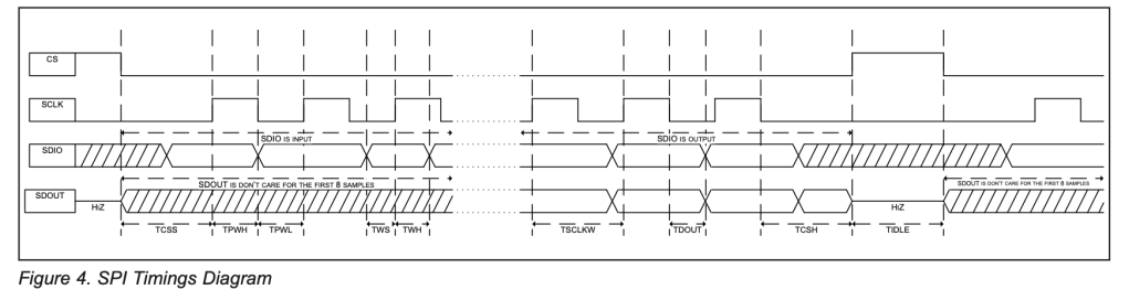
This is more like the diagram we’d expect. It’s a variant of SPI where the PICO (Peripheral In/Controller Out) equivalent pin is named SDIO (Serial Data In/Out). With “IO” in the name, it’s clear this isn’t standard SPI; maybe there is an overloaded function on that signal, meaning the signal is doing double duty. Traditional SPI has unidirectional pins. Some devices allow for optional half-duplex communication modes with SDIO. This reduces the number of pins needed on the controller for the interface.
You can see hatched areas of the signal. These are “don’t care” states.
Before CS(chip select) is asserted and just before we release CS after our data shift, we see that we don’t really care what SDIO is. Similarly, until a command/read request is sent to the peripheral, SDO will be in a state that we are not interested in; it could be high, low, or tristate (high-Z).
We notice that SDIO is changed while SCLK (Serial Clock) is low. Each bit can be either high or low, which is determined by the message content. If you look carefully, you will see that most transitions on SDIO happen between the falling and rising edges.
Most, not all! That second transition is shown as happening with the clock edge. I wonder if that’s a mistake in the drawing? You see a timing reference line for showing clock timing TPWH and TPWL; maybe, during a review of the diagram, someone thought that the SDIO transition should cross on that line. Perhaps I’m overthinking this; after all, look at the setup and hold times for data (TWS and TWH). The diagram implies we don’t have to hold through SCLK’s high time, just around the rising edge. Until we look at the timing information, we won’t know.
That confirms it. We have a TPWH of at least 9ns, but only have to hold our data for 5ns after the clock edge.
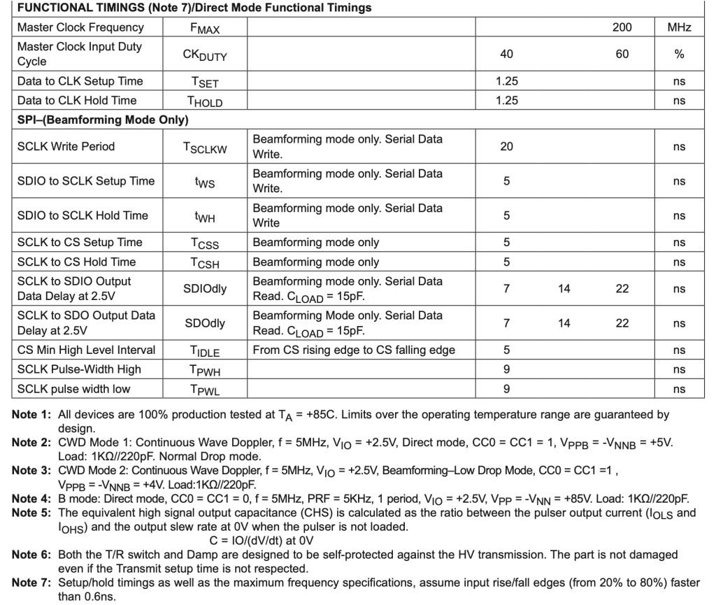
AD7606BBCHIPS
So, that’s a more normal-looking Maxim datasheet. Let’s have a quick look at one from Analog, the AD7606BBCHIPS (DAS with ADC).
This is a very dense diagram. As well as showing timing, it reveals details of the protocol used for the transaction.
Stylistically, this is a little different. Don’t care is shown as a grey region. Gaps in data are represented by squiggles instead of dotted lines.
Our clock polarity is opposite here. That’s allowed. I could write a whole other post about clock polarity and phase (CPOL, CPHA) and the four modes; another area where datasheets never agree on terminology and phrasing.
I see SDI is set up before CS# is asserted. How do I feel about that? I’m not sure, it certainly is unconventional. Again, timing data will let us know if the diagram is correct by examining ts_CS_SCK and ts_SDI_SCK (setup time).
The time between CS# assert and the first data clock is only 2ns. We have to set up SDI at least 8ns before SCK, so yes, if we want to limit our time on the bus, then we set up SDI before we assert chip select.
If we are writing firmware and have a SPI controller in our MCU, we would configure the SPI device, assert CS, then rely on the SPI controller for driving SCLK and SDI and receiving DOUT. If we had only one SPI device and a smart enough SPI controller, it could manage the CS# for us, too.
Back to the Confusing One
So, now we’ve looked at “everyone else”, let’s go back to the one that looks odd.
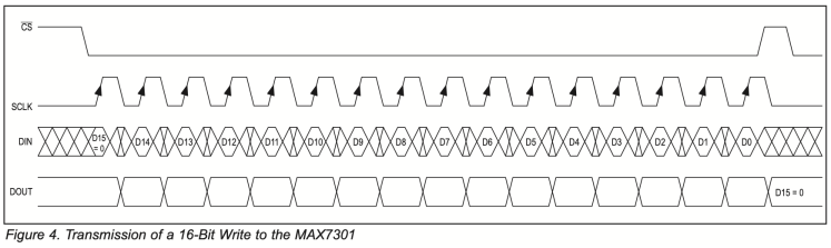
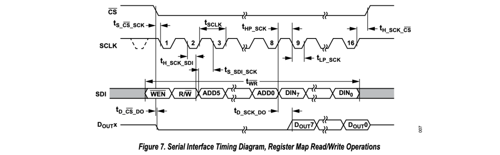
If you’ve ever worked with double data rate (DDR) buses — the kind that latch data on both rising and falling clock edges — this kind of timing diagram might look familiar. You can see that at the midpoint of each clock, there is a transition in DIN.
There’s a second timing diagram. The one above is simply illustrating the protocol; the other examines timing.
It’s more apparent here that, rather than a grey region or parallel stripes, they have used transition crosses to show “don’t care”. The spacing on this diagram allows us to see sustained periods of don’t care outside the critical setup and hold time around the clock edge.
When you see this diagram, you start wondering what the underlying technology is. To me, this looks like what we’d write in Verilog as @(posedge) – meaning the data is captured exactly on the rising edge of the clock. That’s typical flip-flop behavior. When I see the other diagrams, they appear to describe a latch. With a latch, the data must be held in the correct state until the opposite clock edge is reached.
I could try and explain it all here, or I could point you to a brief, well-illustrated article by All About Circuits. It’s been years since I had to concern myself with such details, so I’ll let an expert guide you.
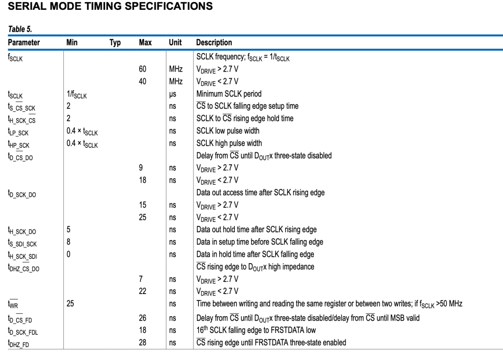
Since we looked at the timing specs for the other devices, it’s only fair to do the same here.
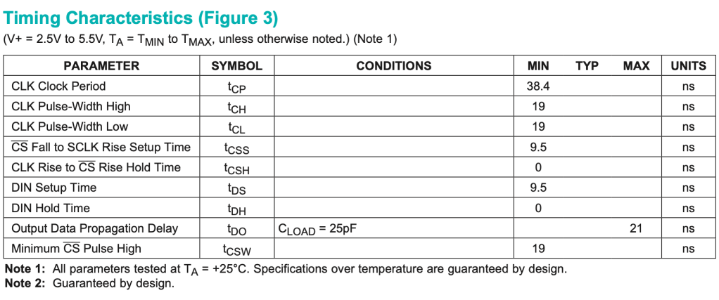
Look at that, tDH is 0ns! Once the clock rises, we’re done! We can release or change the pin ready for the next rising clock already.
Everyone Else Is Wrong!
I know, all those diagrams we’ve been happily enjoying for years are wrong! Outside of setup and hold time, we really don’t care what the value is, or rather, the chip doesn’t.
If the device is truly flop-based and latches data at the clock edge, then we can change as soon as the hold time is complete. If it is a register with flow-through, then we must hold the data steady until the trailing clock edge.
Clarity is the key part of any diagram. They are there to disambiguate text. Although more accurate, the busyness of all the extra “don’t care” information is distracting. Perhaps if a grey fill had been used instead of the crosses that resemble transitions, the diagram would have been less shocking.
Maybe what we commonly see are “idiomatic timing diagrams”. Diagrams that follow a convention that implies a best practice (only transition on clock low) rather than stating the rules (you can transition after the hold time is satisfied).
I can now respect the intent and meaning of the diagram in the MAX7301 datasheet. Does that mean I have to like it? No. Moving forward, I will be a little more mindful of what is being communicated.
Learning To Read Timing Diagrams
I’ve been helping software engineers and junior embedded engineers decode data sheets for some time now. Over the years, I’ve helped many embedded developers — especially those coming from a software-first background — who had been wrestling with timing diagrams. These things aren’t usually taught in school, and vendor docs often assume hardware literacy. So I went looking for better learning resources. I thought I would find some good articles about “how to read datasheets.” Unfortunately, all I found was information geared towards electronics hobbyists, with a focus on electrical properties and gross functionality.
While trying to decode the problematic diagram that was the focus of today’s post, I came across the Rheingold Heavy website and their article on timing diagrams. I think it’s a good primer. I see they also used one of my favourite tools, Wavedrom, to create their illustrations. I hope you get some help from that page.
If you’ve come across a diagram that tripped you up, feel free to share it — I’m always up for adding to the rogues’ gallery, or wall of shame. I’m collecting examples of good and bad diagrams – each one helps me build my illustration skills.
Sources
- MAX7301 datasheet
- MAX14813 datasheet
- AD7606BBCHIPS datasheet
- Edge Triggered Latches and Flip-Flops (All About Circuits)
- Timing Diagram Basics (Rheingold Heavy)
Non-Exclusive Language Policy
Challenged Language
The traditional names for SPI signals have come under scrutiny in recent years, and rightly so. The Open Source Hardware Association (OSHWA) has proposed updated, non-exclusive terminology, which I follow in my blog posts and site content. See OSHWA’s resolution on SPI signal names.
Although not directly relevant to this post, I²C naming has also been challenged. NXP, who still maintain the bus specification, updated their terminology in 2021 – I follow that newer convention as well.
Regional Idioms and Metaphors
Language is very regional. When I first came to the US, I had no idea what the baseball and American football metaphors meant. Likewise, my UK phrasing, idioms, and slang puzzled my new colleagues.
As a writer, I like the full power of my vocabulary; I am mindful of my international audience. Keeping the text light and engaging should not come at the cost of comprehension. Readability shouldn’t mean dry technical verbiage.
Today’s phrases are
“Rogues’ gallery” – Imagine the “top ten most wanted” wall in a police station, photos of the rogues or “baddies”.
“Wall of shame” – Another common phrase to that captures the same idea is “wall of shame”, a place to hang pictures of those who did something wrong.
