It’s not all work with me. Last night I was out to dinner with some friends. One of them, a fellow engineer, knows my fondness for tackling I2C bus issues.
I guess it’s two problems and one factoid.
- Address Conflict
- An SoC (system-on-chip) or SoM (system-on-module) had an embedded I2C target that matched another target in the system.
- Pull-Up Conflict
- Internal 1.8V pull-up blocking other targets on the system with a board level 3.3V pull-up
- SCL Can Be Asymmetrical
- Actually observed to be about 90%
I know, at this point, some of you will be glazing over and moving away, but others will be saying, “I saw that once!” Our other two friends listened with mild amusement as we geeked out for a bit, but mindful of our audience, we got conversations back into more general topics.
Address Conflict with an Internal Device.
This one was presented as something discussed in a job interview. If you ever interview for an electronics engineering or embedded software position, you will be asked about cross-disciplinary debugging that you’ve been involved in. You have a few minutes to discuss your favorite bug hunt.
The candidate talked about a system where one of the targets was responding poorly. In the brief conversation last night, I was given a brief sketch, so everything I say here is based on hearsay and my extrapolation of the facts.
I wasn’t given details of how the bug was uncovered; just the basic context.
The system included a “Qualcomm SoC” and some I2C-connected peripherals on the main board. I know two types of engineers: those who remember the part number to the last digit, and those who remember vaguely which vendor and device type. I fall into the latter camp. I have a terrible memory for numbers, but a good grasp of sequences and architectures. I quoted “Qualcomm SoC” as that was the term my friend relayed.
I’ve worked with quite a few SoCs from vendors like Broadcom, Zoran, Ambarella, ST, NXP, and Atmel. I don’t think I’ve seen any of them have an internal I2C bus. I’ve worked on a couple of ESP32 SoMs, the WROOM and ublox, and know they had SPI, so why not I2C devices on the module?
I am aware of some IMUs, particularly the 9-axis devices, that appear to have multiple dies in the package. Some of these expose I2C and SPI busses, with interesting internal bus bridges where an I2C-only die is fed from a SPI-to-I2C bridge.
The LSM9DS1 9-axis IMU is an example that came to mind. The chip responds to two I2C addresses: one for the combined accelerometer and gyroscope, and the other for the magnetometer.
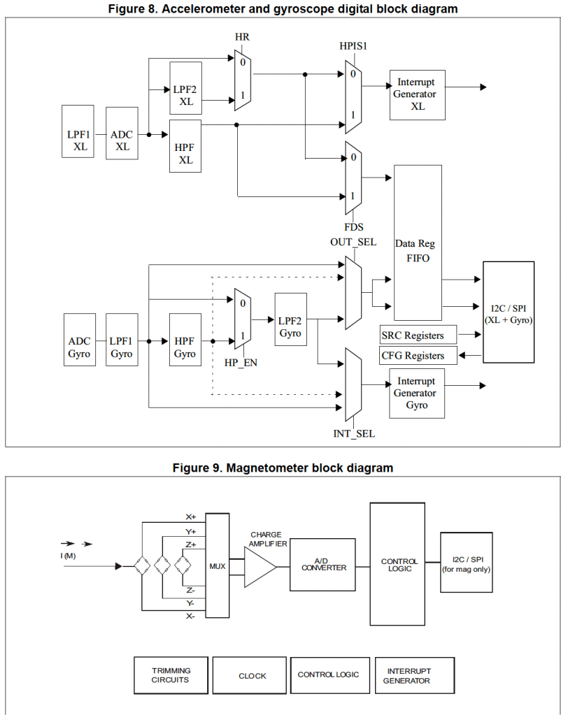
To add to the mix, we see that not only are two addresses exposed, both addresses can be changed by pin strapping to resolve bus conflicts, allowing two of these IMUs to reside on the same bus.
I suspect that the 3-axis and 6-axis devices became combined at some point. Whether this device contains two dies in one package or if the IP is on a single chip, I am unsure. The result is saving space and simplified routing on board, at the cost of slight obfuscation of bus nodes.
The MPU-9250 from InvenSense is a device I have used with interesting bus interfaces. The I2C can be chained through to a magnetometer, or the MPU-9250 can manage the magnetometer for you. With the AUX I2C interface, the bus map is hard to determine just from a schematic review.

The idea of an embedded I2C target in a SoC is not incredible, so the story holds up. Address conflicts are a common issue in systems with multiple I2C devices.
Normally, a diligent schematic review, supported by datasheets, will catch these issues. Once in a while, one slips through the net. This mostly happens when one vendor uses the real 7-bit address and the other uses the 8-bit address. The 8-bit address is (addr << 1)|read_not_write_flag. A rushed review, or poor transcription from datasheet to schematic footnote, can allow these errors to slip through the net.
This is where adding a SoM adds complexity to the schematic and system design reviews. You have to look at the whole SoM in the design review, and make sure you understand any on-module peripherals that are on buses exposed to the main board. With the Espressif WROOM, for example, you will see one of the SPI busses is purely internal, connected to the flash containing executable code. The exposed SPI bus is a second SPI controller on the ESP32.
Pull-Up Conflict
Times have changed. 5v TTL is no longer the only game in town. Wikipedia can tell you more about logic voltage levels. Adjacent technologies can often work together; however, if you have peripherals operating at very different voltages, you’ll want to put level shifters in your circuit.
The example given to me was a device that had a software-configurable internal pull-up to 1.8V that could be disabled by an I2C write. The default was for the pull-up to be enabled.
There were other devices on the bus that operated at a higher voltage level, 3.3V and an external pull-up to 3.3v was provided on the bus.
Until they could set the offending peripheral to not connect its pull-up, the bus was unstable. At the dinner table, I didn’t quite get what the offending level would be. Surely a pull-up to 3.3V would get to 3.3V, even if slowly. This morning’s shower thought was “oh, that’s a classic resistor divider!”
The SCL and SDA lines were connected to 3.3V and 1.8V through resistors. Depending on the ratio of the resistors, we would lie anywhere between the two values. If the two were of roughly equal resistance, we’d see about 2V. Let’s look at that Wikipedia page; there’s a table that shows what we should expect for the CMOS components we are using.
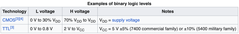
70% of 3.3V is also about 2V. You can see we are at risk of never getting to a logic high as far as the 3.3V devices are concerned.
So, yes, mixing technologies and voltage levels is a tricky situation. Having internal pull-ups is something you cannot catch on a schematic review. Hopefully, your EE reads the datasheets fully.
Asymmetry on I2C Signals
When being told about asymmetric signals on an I2C bus, I was not surprised.
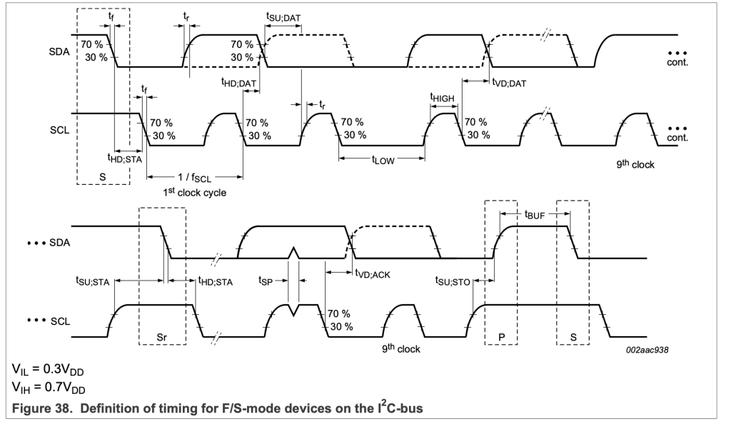
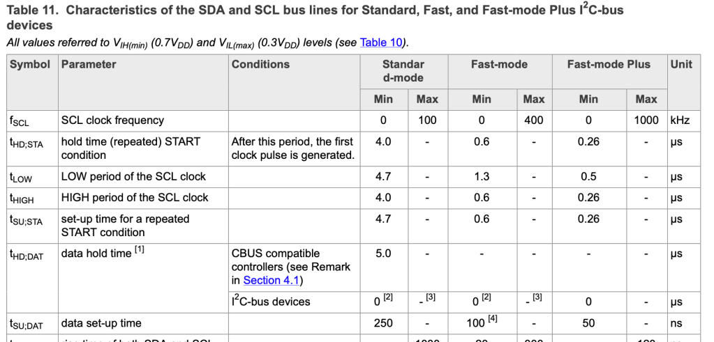
The I2C specification, readily available from NXP, specifies minimum times.
There is a feature, clock stretching, that allows a target to slow down the bus to its speed. I was assured this was not happening.
I have done enough bit-banging on SPI, UART, and I2C buses that I know getting perfect timing is not always possible. But this peripheral was not one of those.
My last thought was, “How was this signal observed?”
The presented timing diagram and table above are from UM10204, the definitive guide to I2C. You can see that the fall and rise times are not expected to be of zero duration. You will see this on an oscilloscope.
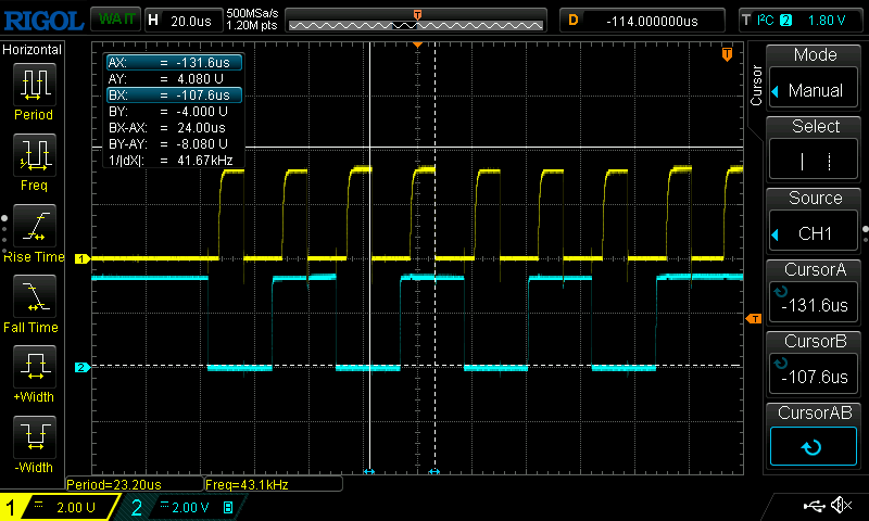
A logic analyzer (or digital channels of your oscilloscope) presents a square wave, showing only when the logic level is high or low. Samples taken along a rising or falling edge, depending on the voltage at the time sampled, could be either. The general rule is that if your signal is above two-thirds full voltage, it’s considered high, but a low is below one-third. If the rise and fall times are significant relative to a bit time, your logic analyzer may display an asymmetrical clock.
If your clock is already asymmetric, with slow transitions, the effect gets amplified.
Another important consideration with logic analyzers is the impact on sampling frequency versus the frequency of the signals being observed. You must sample many times faster than the signal to obtain a true representation. You can get away with 2X; See https://en.wikipedia.org/wiki/Nyquist_frequency for a bit more information.
I Don’t Have The Answers
I know, it seems like I have answers for each of the three scenarios. I don’t. These answers, put together from my experience, are where I’d start looking for each issue. I wasn’t involved in any of the investigations, but the scenarios are familiar enough.
By being aware of common problems, you can quickly triage bus issues. However, a fixed triage list can lead to trying to fit a problem into known patterns. The more scenarios you’ve encountered, the better your odds of identifying the right suspect. My friend and I, both with 30 years of experience in the field, still have those “have you ever seen this” conversations, even with old technology. We still face bug hunts where nothing on Stack Overflow quite matches.
I’ve shared these three scenarios as they are uncommon. If you meet one of them in the field now, you might recognize them. If I can save one person a couple of hours’ effort, then I’ve done my job with this post.

So wrt the i2c pull-up conflict, we were using an STM32 to communicate with an si5395 clock synthesizer IC with other ICs on the same bus. The MCU could communicate just fine to the si5395, but it was unable to communicate with the other ICs. We measured the logic high on the signals at a surprising 2.3V. I think (could have been a different voltage, but let’s go with this for sake of argument). 2.3V is surprisingly very close to the .7*3.3V = 2.31V threshold that we need to surpass for I2C
The IC has a selectable i2c VDD_IO voltage, but it defaults to 1.8V and is selectable only with a write to an internal register.
I scoured the datasheet and family reference manual which explicitly says there is no pull up on the SCK and SDA signals and recommends an external 4.7K ohm pull up on both.
However these signals are dual purpose signals; we selected the i2c function with a pull up on the I2C_SEL pin. It does make one wonder if there are leakage paths in the IC when you have dual purpose functionality like this.
The PCB has a 10k ohm external pull up (not the recommended 4.7K ohm) on both signals. Using some voltage divider math I suspect there is an internal 47K ohm pull to VDD internal to the IC (the IC requires VDD = 1.8V and VDDA = 3.3V).
If we had used the recommended 4.7K ohm pull up rather than 10K ohm, the logic high voltage would be around 2.55V, well above the logic high threshold of .7*3.3 = 2.31 that the other ICs on the bus require.
In this case the workaround was to program the si5395 voltage select register before trying to communicate to any of the other ICs on the bus. This brought the open drain i2c signals back up to the expected 3.3V. After this we were able to communicate to the other ICs.
And yes, before adding this note I did search the internets for any clues about this IC misbehaving. No joy.
The sad thing is that I debugged this the first time with one colleague, then forgot about it. Another colleague six months later ran into it on a different board and then picked up the trail after glancing at a white board where we had drawn the very same circuit. We have it documented in our wiki now 🙂
LikeLiked by 1 person
Thanks for the info.
I took some time last night to read up on the si5395. I could see a time where there could be a fight on SDA, but that would involve.
– I2C_SEL being set low to enter SPI mode
– Setting the SPI to 3 wire mode
– clocking in data enough that a read command was detected
At that point, the si5395 would be driving the SDIO line as push-pull.
That’s a way to get to the conflict, but that would take a very unfortunate sequence. I am assuming I2C_SEL was pulled high, and not under the control of the STM32, so I doubt you could get in that state.
LikeLike
Correction: I suspect 4.7K ohm internal pullup, not 47K ohm.
LikeLiked by 1 person