- About today’s blog post
- GPIO test point
About today’s blog post
I am cheating today. I am sharing a “work in progress” chapter from my book.
I spent considerable time over the last 24 hours polishing this chapter. It still needs a run through a grammar checker, though. I believe it deserves more images, too. However, I am not embarrassed to share it in its current state.
I am going to probably also add this content to my wiki. I thought I would share it here with the threefold purpose of teasing the book, providing technical content, and saving me the effort of writing this week’s blog entry. Any feedback here would be welcome too; I need to make sure I am giving worthwhile content in a readable format.
Of course I’ve been writing in markdown, and have to convert for here, and import the images, so it’s not a freebie, just bargain basement pricing.
GPIO test point

One of the most valuable aids for debugging an embedded system is also the simplest; a dedicated GPIO test point.
Test points, in general are convenient places on the circuit board to probe signal. There are various forms, such as a pad, simple post or loop. Special connector like banana jack or BNC connector may be utilized. These test points are placed strategically, and are on signal that are part of the system.
The debug test point is a special software-controlled test point that does not provide any part of the system’s functionality but is dedicated to debug output.
Having a direct output from your MCU to a test point allows for many things, including system alive, progress indicator, critical timing and failure codes. It is invaluable in debugging boot code and start up sequences, where problems occur before a terminal session can begin.
You can monitor this test point with a variety of tools. If it is fitted with an LED you can even observe with the naked eye. The LED is a good way of presenting a heartbeat, activity indicator or a POST (power on self test) code. A lot more information about the system can be gathered is the test point is used in conjunction with an oscilloscope.
Depending on resources available, if this test point can be controlled by PWM hardware in your MCU, then you can get a lot more information from your system.
Uses of a GPIO test point
- milestone – a progress indicator.
- heartbeat – a visible blink at a uniform rate.
- POST/ERR code – a visible blink pattern.
- UART – bit banged serial data interface.
- execution timing – how long was a function or state active.
- latency timing – time taken from an event to completion.
- idle time monitoring – what is the real CPU utilization.
Selecting a GPIO pin for the test point
The best GPIO test points are dedicated for this function, and designed into the system.
There are a few rules for selecting the test point GPIO when designing the schematic.
- Direct processor output.
- Accessible to all cores in SoC.
- Does not consume a valuable pin.
To be frank, on a very small system, you may not have enough pins for a dedicated test point. You may have to disable part of your system, and re-purpose a GPIO not involved in the debug effort as test point.
There are also rules for re-purposing another pin after the board is made.
- Direct processor output.
- Has an accessible pin, pad, via or trace.
- Repurpose signal in a non-critical subsystem.
Direct processor output
When I first review a schematic for a new board I always look for a dedicated GPIO test point. There are reasons why the designer may not have included one. If there are any unused GPIOs on the MCU, then you should lobby for a dedicated test point.
A dedicated test point only takes two writes to configure and set, namely a write to the port data register, then to the port configuration register. Even in assembly code this is not daunting.
; Assembly code for 68HC11 - Setting bit 2 of PORTA and DDRA
; Set bit 2 of the Data Register of Port A
    LDAA    $1000     ; Load the current value of PORTA into Accumulator A
    ORAA    #%00000100 ; Set bit 2 (counting from bit 0 as the LSB)
    STAA    $1000     ; Store the modified value back into PORTA

; Set bit 2 of the DDR of Port A to configure it as output
    LDAA    $1001     ; Load the current value of DDRA into Accumulator A
    ORAA    #%00000100 ; Set bit 2 to 1 to configure as output
    STAA    $1001     ; Store the modified value back into DDRA
The register address shown may vary between devices.
- Port A Data Register (PORTA): e.g., address $1000
- Port A Data Direction Register (DDRA): e.g., address $1001
When even the simplest GPIO expander is used, access to the IO is still much more complex to use than a direct pin. GPIO expanders may be placed on the exposed address/data bus, SPI, I2C or similar busses. The test point would require the associated bus and GPIO expander to be properly configured and well behaved before it could function as a test point.
Once the expander is working, the number of instructions to execute to change the test point would be greater, adding to risk timing sensitive code, especially when using the test point in interrupt handlers.
Our preference for least invasive test is therefore a dedicated GPIO.
Accessible to all cores
Some SoCs have multiple discrete cores. A common arrangement is to have a lightweight core that can handle low power and system wake-up tasks, then a larger CPU for main processing.
When you have such a system you will see that not all GPIOs can be reached by the low power CPU when the system is in a low power state. Indeed, much of the bus, and many peripherals may be un-powered or un-clocked at this time.
If you are not pin constrained, each CPU can have its own test point pin. If not, then find a common pin, and make sure that only one controller at a time is trying to use it.
Does not consume a valuable pin
GPIO pins often have an option to be a simple IO pin, or can be controlled by a functional block within the MCU.
When designing the system you will allocate the special purpose signals to take advantage of the MCUs internal hardware when possible. This includes USART, SPI, I2C, ADC, PWM controllers. Each block will map to a group of pins. Sometimes a signal could be switched to one of several package pins. Pin selection is a non-trivial task.
After special functions have been assigned, the hardware designer will select direct GPIO for the highest usage and most speed critical signals. Once pins have been exhausted, the lower priority GPIO signals will be moved to a GPIO expander. It is important to recognize the debug test point is one of the higher priority outputs.
Borrowing another IO for the test point
As stated above, a dedicated test io may be a luxury that your hardware design cannot afford. You can borrow a pin as a test point, but you must find a pin that
- is under control of software that can be disabled without impacting your debug effort.
- you can get to physically.
- does not adversely impact system performance.
Non-critical donor pin
If you have no spare pins, and you need a test point, then you must temporarily disable one of your interfaces to allow for a test point. Knowing which subsystem is not impacting the bug is a learned skill, and requires knowledge of the whole system.
When first implementing a subsystem, you will be wanting to develop the lower layers in isolation, so you are free to disable everything else.
If you are integrating, then you may have an easy choice. For example, if you are developing a camera, and you want your I2S CODEC output to align with your video signals, the the IMU for image stabilization (IS) is a non-critical sub-component. In this instance you can re-use the IMU only interface lines for your test point. Conversely, if you were debugging the IS, then you need the IMU, but the audio CODEC is non-critical.
For your system to work you may need to operate the full system. When trying to find a test GPIO you might find something that you can “live without” for a few days. Good candidates are user feedback LEDs and buzzer outputs.
I agree, having a crackly sound over the buzzer is not optimal, nor is having a mode LED not tracking the mode, but if you really need the test GPIO, then sacrifices have to be made.
You will have to make sure that the pin is actually under your control. You will get poor feedback if your test point is trying to perform its usual 1 Hz blink while also showing entry to a sub-routine. Other output pins might have adverse impact. Chip select signals, for example, are a poor candidate, as then active in the select state then the peripheral under control will start reacting to other signal.
Was the pin an output before you borrowed it? An input, or in/out signal may toggle as the result of other circuitry outside the MCU. This would give spurious edges and bad state, making your test output unusable.
Physically accessible/Exposed to test equipment
When trying to find an extra test point on an existing board, you must select a signal that is accessible.
In the past you were sure of an IC pin or lead to connect to. Some packaging, like DIP (dual inline package) had very accessible pins. Packaging like BGA (ball grid array) have no visible pins, as the contact points, the balls, all lie on the underside of the component.
Traces between BGA packages may be blind, that is, they run entirely on an internal board layers. To determine if a signal can be used as a test point, you will have to refer to your schematic and layout
You should look for any of the symbols for
- test point
- IC pin
- Discrete component such as capacitor, resistor
that may be attached to.
If the signal goes between hidden pins you will have to look at the layout, looking for where the trace comes to a surface layer, if ever.
Vias, where the trace moves between layers, are slightly easier to hold a scope probe against than a trace as there is a small drill hole that make a nice detent to rest against.
For a more permanent test point look to something big enough to solder a wire to.
Placing the GPIO test point
Though ultimately the board designers responsibility, you may influence some of the decisions made in test point placement. You may also find that your preferred location for a test point is not possible.
Mechanical considerations
This test point can be used at every stage of development, and will often be subject to long term continuous monitoring, and therefore should be something more than a pad. A standard header post works well with logic analyzers and MSO digital channels. Consider using a loop to attach the a j-hook probe, as you find on an oscilloscope. There should be an accompanying ground pin nearby.
You may suggest this test point and ground be placed near the edge of the board. Since this is a test point that may be always attached, the test leads to it would droop across the board, getting in the way of other test points you may wish to probe.
Though a lot of boards have an obvious top side, where everything connects, there are some times where a board is busy on both side. For example, you may have user buttons and displays on one side, but all the connectors on the back. Will you be wanting to have all your cable plugged in and facing away from you while you want to probe test points on the side with the UI (user interface)?
Small form factor boards may come with a breakout board, connected by an umbilical to the main board. None of the test features being present on the actual product, other than the interface between the two boards. Your debug test point will probably be on the breakout board, but this might be a good exception to keep on the final product, especially if an debug or heartbeat LED is associated with it.
Electrical considerations
When laying out a circuit board, careful attention is paid not only to how components interconnect, but also how the signals propagate through and around the traces. High frequency signals can cause electromagnetic interference, with signals coupling onto adjacent circuits. T-junction in wires can cause issues, and dead end trace become antennae which increase the RF noise around a board. Test points, especially if not on the direct path between two points, can increase capacitance, reflections and other anomalies.
Add a blinking light
If the test point is only to be used for crude timing, an LED can be added. The LED heartbeat is a quick visual check that either the main loop, or the watchdog reset is periodically visited. Even if the TP is used for a UART, the LED would flicker with data bursts, even if a terminal was not connected.
LEDs do impact the electrical characteristics of the test point output. Work with your EE on getting an appropriate visual indicator that will work with all your test cases.
If you only want an LED some times, and not always, use of jumpers can isolate the LED, or you could make a plug in LED that connects between the test point and VDDIO or ground, again, your EE will advise you about how this can be done.
While on the topic of LEDs, a power good LED can provide valuable insight. You may only be able to negotiate for these on early prototypes, but I have seen an indicator on every power rail for rack mounted systems where they are essential for field service technicians to identify problems.
Using the GPIO test point
Why use a GPIO pin when I have a debugger and a terminal monitoring a UART?
GPIO test points are extremely lightweight, and minimally invasive in monitoring a system.
When debugging system bring up, a couple of writes to the GPIO block will be able to show you “are we there yet” even before you have had a chance to set up your serial port for transmitting. Remember also, some tools, like the ESP-Prog programmer/debugger from Espressif take some time to swap from program to UART monitor functionality. In this non-zero time the boot session could complete before a terminal session is available to view.
Using a debugger can tell you where you got to, but unless you breakpoint at the code in question you will not know if you passed through that point. Stopping at a breakpoint in embedded code may cause a fatal system error, especially when communicating with peripheral components, requiring a restart of the system, rather than a resume.
To measure timing with print statements requires executing a print. Prints take many cycles to complete. You may record the start and end time to variables, and then print after the event, but still the prints will impact overall system performance.
The biggest win of the GPIO test point is the ability to use it within an ISR. If your processor has a bitset function, then it is extremely fast, but even if you have to read the GPIO data register, OR the bit for the test point, and write it again, this is still very fast.
Depending on your system, you may find the only way to truly measure the timing from the release of reset to a milestone mark within the boot code, or start of main execution loop, is by way of the test point. A lot happens between reset and the system actually counting its internal ticks.
Milestone
Sometimes you want an non-invasive “I’m here”, or “This happened” signal. In the days before on board debug capability, turning on the test point LED at a milestone was key indicator of what succeeded in boot code. This is probably not of great importance these days, but it was once our only way of seeing progress.
In a modern system you might use a milestone to show if something has happened. Again, this is more likely for a system where you have limited system visibility. You could set up a milestone in an error handler, and leave the system for a long term test, say over the weekend. When you come in on Monday morning you can see if the error happened at all.
This will yield an “at least once” metric.
Heartbeat
Typically a heartbeat will have an associated LED. The heartbeat is a regular interval blink. The heartbeat is an indication of continued activity.
A heartbeat does not have to be a 1Hz 50% duty cycle pulse. Heartbeat can carry some other information, such as active, sleeping or fault. Typically a heartbeat will be something you can see in a quick glance, which is why 1hz is a good starting point.
You may be tempted to use a hardware counter timer block to control the heartbeat. This independent block of hardware can be set up as free-running. Your heartbeat will still pulse, even if the software has ground to a halt.
In single threaded code, you will be able to blink within your main loop. In a multitasking system, you will use some level of activity monitor to control the blink pattern depending on system health.
For sleep states a slower frequency is used. Since sleep states are associated with low power consumption it’s common to have the LED flash for a fraction of a second every few seconds. Anything more than 30 seconds between blink, it will be hard to notice. Have you ever watched the status LED on a smoke detector? They blink for a fraction of a second every minute.
For error states a faster blink is often used. If the error is a fatal error, then normal operation would cease. At this point the blink could be something other than a simple square wave. Maybe once per second you emit an error code, much like morse code.
State or task identifier
There is a cool trick when the test point can be connected to a PWM controller, or a DAC. You can encode the current task ID or the current state. With a PWM, you can measure the duty cycle as an identifier. If the output is smoothed to a voltage, then you will see steps to discrete voltages as the states transition, of the OS context switches between tasks. This is an advanced trick which I have only applied once in my career, but it helped monitor real time state transitions while I was hunting down an interrupt response latency issue.
POST and error codes
POST (power on self test) should conclude with no errors and allow normal operation to continue. Each error that can occur within the start up of the devices has a unique code associated with it. It is not uncommon to show these diagnostic codes as a blink pattern on the test point.
Error codes are not limited to power on self test. Any time BIST (built in self test) catches an error, an error code can be emitted. You may be familiar with beep codes from the BIOS of your computer, which is an audible form of a POST code.
Serial output
You can implement a slow speed serial connection on a single GPIO pin. You can bit-bang a message onto the bus.
This is expensive in system resources (CPU and bus bandwidth), more so than a dedicated UART controller. The timing may not be close to the speed of a UART, but you can capture the pulse train on an oscilloscope or logic analyzer, and reconstruct the message.
Some MCUs do not have a UART or on-board debug, so this would be a last recourse way to tell the outside world what went wrong.
Execution timing
For system profiling you will need accurate timing analysis. The use of a UART to send timing information to the outside world will be costly in a resource constrained system, and intrusive in some contexts.
To critically measure a function’s execution time you would set the state of the test point on entry, and clear it on exit. Note, this testing will not work for re-entrant functions as you are introducing a critical shared resource, the GPIO pin.
Using your oscilloscope you can see two important measurements.
- execution time
- frequency of execution
To see the execution time, you measure the time from set to clear of the pin. With most oscilloscope you can set for a recurring trigger, and see every event. Adjust the display persistence so that the ghost image of the previous instances are visible. You will see that the active time for the function is not always exactly the same. A long running test with infinite persistence, will reveal best case and worst case timing.
If there is significant difference between average and worst case, then you are probably seeing the impact of a task switch mid function.
To see how often a function is called, you measure the time between successive leading edges where you set the test point.
Latency timing
The elapsed between an event and the response is critical in system performance. We need to know we are able to capture all events and process them.
Interrupt latency refers to the time between an interrupt being raised and the interrupt service routine responding. By setting our test point within the interrupt handler we can see how long it takes to respond to an interrupt.
The test point can either be cleared within the interrupt handler, the interrupt service routine, or a thread that will handle a larger transaction in response to the interrupt.
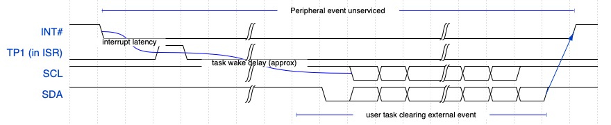
For example, when an IMU has a sample ready, it raises an interrupt. The ISR will record that data is ready, and unblock the IMU worker thread. When the scheduler allows the thread to run, then a bus transaction to the IMU will happen. This will typically release the interrupt signal from the IMU to the host. Once the bus read of IMU data is complete, only then is the data ready for use internally. This accumulation of delays is the overall latency. You can use the test point to measure how long it takes to get to any point in this chain of events.
Idle time monitoring
The test point can be used to see how long we spend in the idle task.
Knowing when the system is idling will help us identify when a system is at risk of becoming overloaded. It can also identify if we can employ more effective power strategies.
Manipulating the GPIO test point
There are a few simple rules when it comes to writing to the test point.
- Do not disturb other pins in the pin group.
- Make it as fast as possible.
You will typically want the functions
	// one time setup
	config_testpoint()

	// For use in normal code
	// 1. Enter critical,
	// 2. Read data reg, modify bit, write data reg
	// 3. Exit critical
	set_testpoint()
	clear_testpoint()
	toggle_testpoint()

	// For use in interrupt code
	// Read data reg, modify bit, write data reg
	set_testpoint_isr()
	clear_testpoint_isr()
	toggle_testpoint_isr()
Since we are typically performing a read/modify/write sequence, we must have exclusive access to the IO register. This is done by disabling interrupts for the time taken to update the pin. Within an ISR we already are in a protected execution mode, and we should not use the enter_critical() and exit_critical()` functions. Hence, we need two flavours of the test point update functions.
To reduce function call overhead, you may want to consider use of the inline directive, or implement these as macros.
Toggle is useful for heartbeat, and for measuring between successive calls to function entry. Set/clear pairs are good for start and stop.
You may also want a “pulse” function. You must be careful, if the pulse is too short and the interval between pulses too long, you might have trouble capturing short pulse while seeing the interval on the scope.
Vendor supplied GPIO functions should suffice, if not your high level language should not be limiting. Try to avoid resorting to assembly language, unless this is an assembly language project.
